 欢迎来到上海巨纳科技有限公司网站!欢迎来到上海巨纳科技有限公司网站!
13761090949


详细介绍
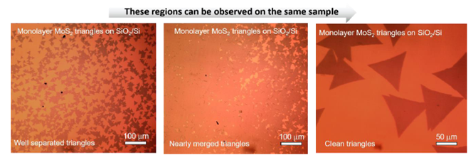
Isolated monolayer thickness MoS2 are grown onto SiO2/Si substrates. This particular product contains monolayer thickness MoS2 triangular flakes randomly distributed across SiO2/Si substrate. While some regions reach continuity with coalesced MoS2 triangles, this sample contains well-separated triangles for advanced spectroscopy, microscopy, and electronic measurements. Synthesized monolayer MoS2 triangles are highly luminescent and Raman spectroscopy studies also confirm the monolayer thickness. Overall, MoS2 monolayer thickness triangles are more luminescent compared to MoS2 triangles grown onto sapphire substrates.
Sample Properties.
Sample size | 1cm x 1cm square shaped |
Substrate type | Thermal oxide (SiO2/Si) substrates |
Coverage | Isolated and Partially Merged Monolayer Triangles |
Electrical properties | 1.85 eV Direct Bandgap Semiconductor |
Crystal structure | Hexagonal Phase |
Unit cell parameters | a = b = 0.313 nm, c = 1.230 nm, α = β = 90°, γ = 120° |
Production method | Atmospheric Pressure Chemical Vapor Deposition (APCVD) |
Characterization methods | Raman, photoluminescence, TEM, EDS |
Specifications
1) Well-separated MoS2 domains across SiO2/Si chip.
2) One centimeter in size. Larger sizes up to 2-inch wafer-scale available upon requests.
3) Atomically smooth surface with roughness < 0.1-0.2 nm.
4) Highly uniform surface morphology. MoS2 triangles are scattered across sample
5) 99.9995% purity as determined by nano-SIMS measurements
6) Repeatable Raman and photoluminescence response
7) High crystalline quality, Raman response, and photoluminescence emission comparable to single crystalline monolayer flakes.
8) SiO2/Si chips but our research and development team can transfer MoS2 triangles onto variety of substrates including PET and quartz without significant compromising of material quality.
9) MoS2 monolayer triangles do not contain intentional dopants or defects. However, our technical staff can produce defected MoS2 using α-bombardment technique.
Supporting datasets [for Monolayer MoS2 Triangles on SiO2/Si]
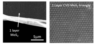
Transmission electron images (TEM) acquired from CVD grown MoS2 isolated triangles on SiO2/Si confirming highly crystalline nature of monolayers
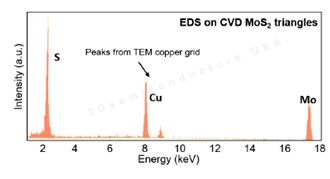
Energy dispersive X-ray spectroscopy (EDX) characterization on CVD grown MoS2 isolated triangles on SiO2/Si confirming Mo:S 1:2 ratios
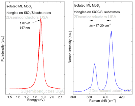

Room temperature photoluminescence spectroscopy (PL) and Raman spectroscopy (Raman) measurements performed on CVD grown MoS2 isolated triangles on SiO2/Si Raman spectroscopy measurement confirm monolayer nature of the CVD grown samples and PL spectrum display sharp and bright PL peak located at 1.85 eV in agreement with the literature.
产品咨询
联系我们
上海巨纳科技有限公司 公司地址:上海市虹口区宝山路778号海伦国际大厦5楼 技术支持:化工仪器网扫一扫 更多精彩

微信二维码

网站二维码
