 欢迎来到上海巨纳科技有限公司网站!欢迎来到上海巨纳科技有限公司网站!
13761090949


详细介绍
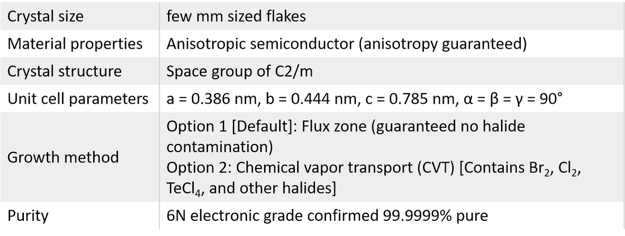
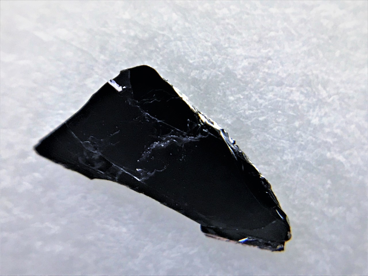
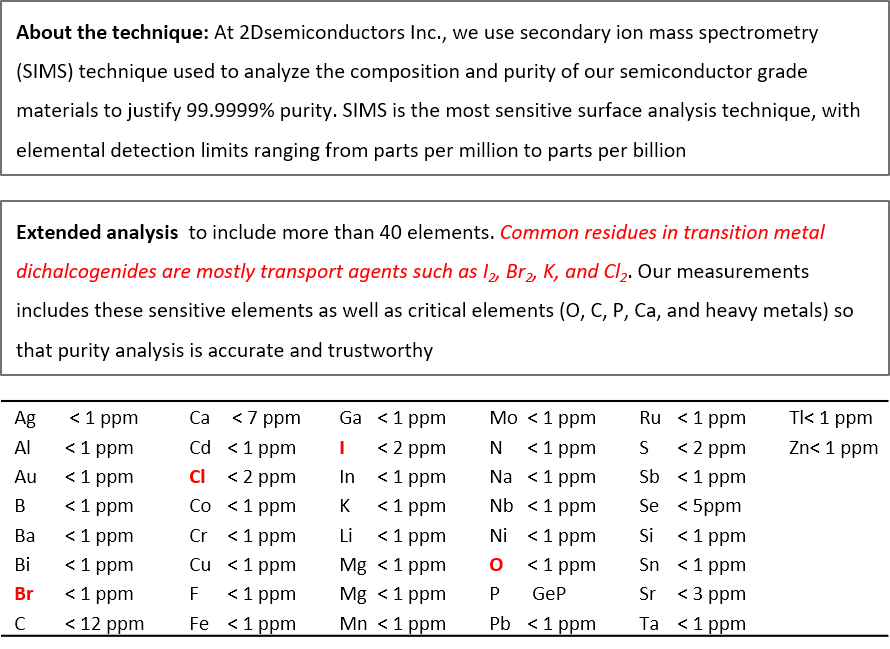
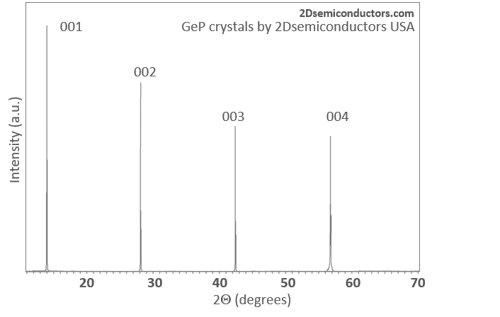
GeP has highly anisotropic dispersions of band structures, with a layer-dependent indirect band gap from (theoretically predicted) 1.68 eV of monolayer to 0.51 eV of bulk. GeP is an anisotropic semiconductor much similar to GaTe monoclinic structure. Our single crystal GeP (Germanium phosphide) crystals come with guaranteed optical, electronic, and structural anisotropy. They are developed at our facilities using state-of-art flux zone techniques. Each growth takes close to three months to provide you perfected crystals that does not contain any halides. Each crystal is highly crystalline, oriented in 0001 direction, and easy to exfoliate. Our R&D staff takes characterization dataset in each sample piece to ensure structural, optical, and electronic consistency. Please also see our GeS, GeSe, GeTe, GeAs, GeP, and Ge-based solutions.
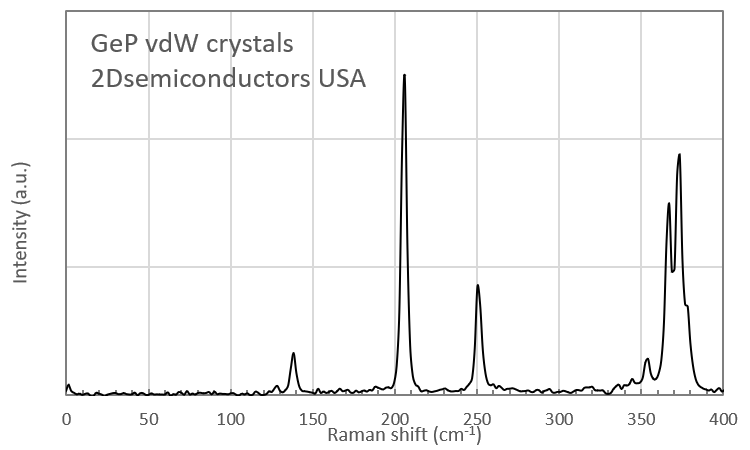
Characteristics of vdW GeP crystals
产品咨询
联系我们
上海巨纳科技有限公司 公司地址:上海市虹口区宝山路778号海伦国际大厦5楼 技术支持:化工仪器网扫一扫 更多精彩

微信二维码

网站二维码
