 欢迎来到上海巨纳科技有限公司网站!欢迎来到上海巨纳科技有限公司网站!
13761090949


详细介绍
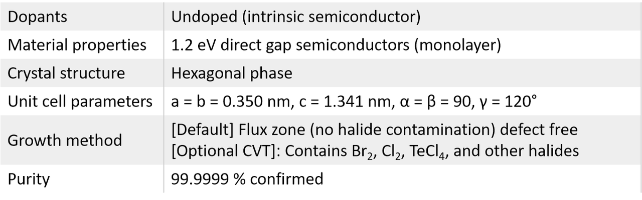
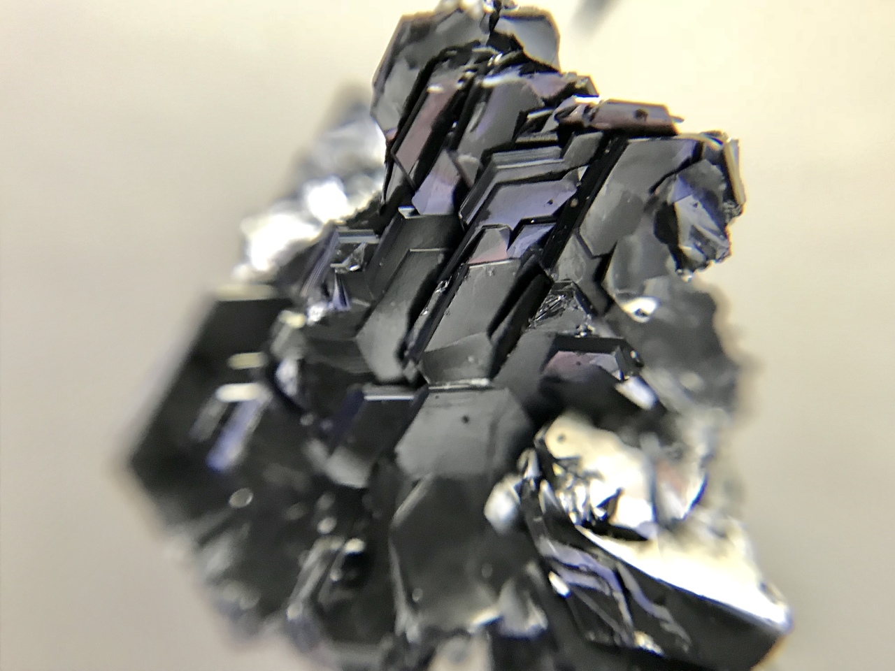
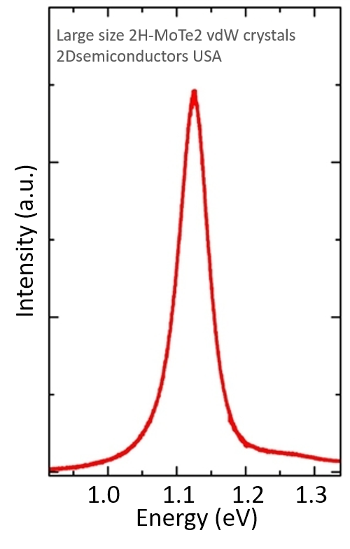
2H semiconducting phase of MoTe2 crystals contain layers that are stacked together via van der Waals interactions and can be exfoliated into thin 2D layers. Our large size 2H-MoTe2 vdW crystals are treated as gold standards in 2D materials field. They come with guaranteed valleytronic performance, clean PL spectrum, perfect crystallization, and defect free structure. Our MoTe2 crystals are synthesized two different methods (flux zone and chemical vapor transport). While flux zone provides extremely clean MoTe2 crystals, CVT method often introduces halide contaminants. For comparison between these tow methods, please see the information below. If your research needs electronically doped MoTe2 crystals, please contact us.
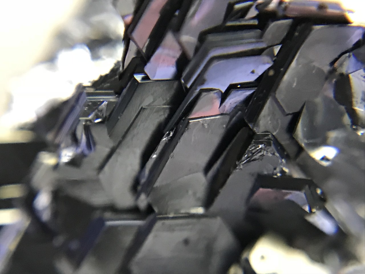
Characteristics of 2H-MoTe2 crystals from 2Dsemiconductors USA
Growth method matters> Flux zone or CVT growth method? Contamination of halides and point defects in layered crystals are well known cause for their reduced electronic mobility, reduced anisotropic response, poor e-h recombination, low-PL emission, and lower optical absorption. Flux zone technique is a halide free technique used for synthesizing truly semiconductor grade vdW crystals. This method distinguishes itself from chemical vapor transport (CVT) technique in the following regard: CVT is a quick (~2 weeks) growth method but exhibits poor crystalline quality and the defect concentration reaches to 1E11 to 1E12 cm-2 range. In contrast, flux method takes long (~3 months) growth time, but ensures slow crystallization for perfect atomic structuring, and impurity free crystal growth with defect concentration as low as 1E9 - 1E10 cm-2. During check out just state which type of growth process is preferred. Unless otherwise stated, 2Dsemiconductors ships Flux zone crystals as a default choice.
Partial List of Publications Using This Product
Y. Li et. al. "Room-temperature continuous-wave lasing from monolayer molybdenum ditelluride integrated with a silicon nanobeam cavity"
Nature Nanotechnology volume 12, pages 987–992 (2017)
Control of Exciton Valley Coherence in Transition Metal Dichalcogenide Monolayers, Phys. Rev. Lett. 117, 187401 (2016)
Tony Heinz Team "Optical Properties and Band Gap of Single- and Few-Layer MoTe2 Crystals" Nano Letters 2014, 14, 6231−6236
Physical origin of Davydov splitting and resonant Raman spectroscopy of Davydov components in multilayer MoTe2; Q. J. Song, Q. H. Tan, X. Zhang, J. B. Wu, B. W. Sheng, Y. Wan, X. Q. Wang, L. Dai, and P. H. Tan; Phys. Rev. B 93, 115409 (2016)
Indirect-to-Direct Band Gap Crossover in Few-Layer MoTe2; Ignacio Gutiérrez Lezama et. al. Nano Letters 2015, 15 (4), pp 2336–2342 DOI: 10.1021/nl5045007
Measurement of the optical dielectric function of monolayer transition-metal dichalcogenides: MoS2, MoSe2, WS2, and WSe2, Yilei Li, Alexey Chernikov, Xian Zhang, Albert Rigosi, Heather M. Hill, Arend M. van der Zande, Daniel A. Chenet, En-Min Shih, James Hone, and Tony F. Heinz; Phys. Rev. B 90, 205422 (2014)
M. Yankowitz et. al. "Intrinsic Disorder in Graphene on Transition Metal Dichalcogenide Heterostructures" Nano Letters, 2015, 15 (3), pp 1925–1929
H. C. Diaz et.al. "Molecular beam epitaxy of the van der Waals heterostructure MoTe2 on MoS2: phase, thermal, and chemical stability" 2D Materials, Volume 2, Number 4 (2015)
S. Vishwanath et. al. "MBE growth of few-layer 2H-MoTe2 on 3D substrates" Journal of Crystal Growth, 482, Pages 61-69 (2018)
产品咨询
联系我们
上海巨纳科技有限公司 公司地址:上海市虹口区宝山路778号海伦国际大厦5楼 技术支持:化工仪器网扫一扫 更多精彩

微信二维码

网站二维码
