 欢迎来到上海巨纳科技有限公司网站!欢迎来到上海巨纳科技有限公司网站!
13761090949


详细介绍
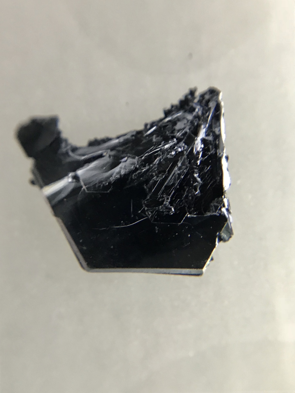
14 years of growth optimization lead to our flawless n-type WSe2 crystals through Au or Re doping: They are simply treated as gold standards in 2D materials field. Our n-type WSe2 crystals are doped with Re or Au atoms at ~1E17-1E18 cm-3 range. However, if your research requires other types or concentration of dopants please contact us. Intentionally doped WSe2 crystals from 2Dsemiconductors are known for its superior valleytronic performance, perfect crystallization, defect free structure, extremely narrow PL bandwidths, clean PL spectra (free of bound exciton shoulders), and high carrier mobility. Thousands of scientific articles have cited us and used these crystals for scientific accuracy and clean signals. Please also see our n- and p-type WSe2 crystals doped with Au, Re, Nb, or other transition metal atoms. Please note that doping into TMDCs greatly reduce the crystallization time (growth speeds), thus electronically doped TMDCs measure smaller than undoped (intrinsic) TMDCs.
Typical characteristics of WSe2 crystals from 2Dsemiconductors
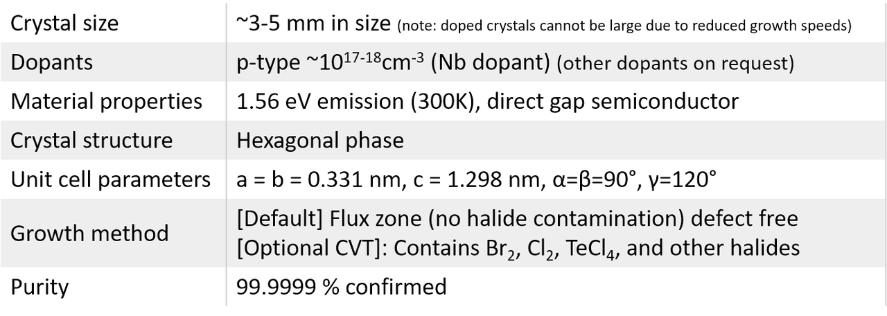
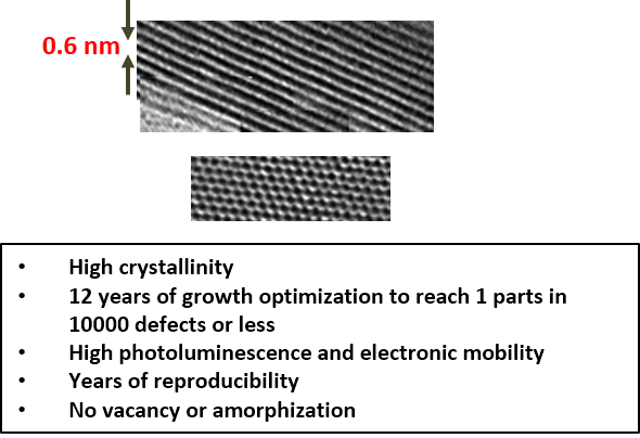
Growth method matters> Flux zone or CVT growth method? Contamination of halides and point defects in layered crystals are well known cause for their reduced electronic mobility, reduced anisotropic response, poor e-h recombination, low-PL emission, and lower optical absorption. Flux zone technique is a halide free technique used for synthesizing truly semiconductor grade vdW crystals. This method distinguishes itself from chemical vapor transport (CVT) technique in the following regard: CVT is a quick (~2 weeks) growth method but exhibits poor crystalline quality and the defect concentration reaches to 1E11 to 1E12 cm-2 range. In contrast, flux method takes long (~3 months) growth time, but ensures slow crystallization for perfect atomic structuring, and impurity free crystal growth with defect concentration as low as 1E9 - 1E10 cm-2. During check out just state which type of growth process is preferred. Unless otherwise stated, 2Dsemiconductors ships Flux zone crystals as a default choice.
产品咨询
联系我们
上海巨纳科技有限公司 公司地址:上海市虹口区宝山路778号海伦国际大厦5楼 技术支持:化工仪器网扫一扫 更多精彩

微信二维码

网站二维码
