 欢迎来到上海巨纳科技有限公司网站!欢迎来到上海巨纳科技有限公司网站!
13761090949


详细介绍
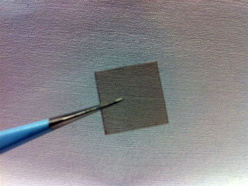
An ideal substrate – template for two-dimensional (2D) materials to eliminate ripple, surface roughness, and doping (charge transfer) effects. It has been develop at our facilities in the last 6 months. Currently, highest quality in the commercial market rated at V1 and higher grade. It is ready for exfoliation onto various substrates. It has a highly-perfect basal cleavage yielding remarkably-thin laminæ (sheets) which are often highly elastic and atomically flat surfaces. It can be isolated to monolayers similar to our other 2D products. This product is an ideal material for 2D heterostructure studies and yielding atomically flat graphene, MoS₂, and other transition metal dichalcogenides. Owing to its surface flatness, transferred 2D materials are surprisingly flat. Perfect product to compliment on your 2D materials research.
Possible applications:
Substrates to 2D materials
2D heterostructure studies
STM – AFM applications
Molecular detection – binding
Ultra-low friction studies
Materials science and semiconductor research
产品咨询
联系我们
上海巨纳科技有限公司 公司地址:上海市虹口区宝山路778号海伦国际大厦5楼 技术支持:化工仪器网扫一扫 更多精彩

微信二维码

网站二维码
